
|
|
8085A
|
The Intel 8085A is a new generation, complete 8 bit parallel central processing unit (CPU). Its instruction set is 100% software compatible with
the 8080A microprocessor, and it is designed to improve the present 8080's performance by
higher system speed. Its high level of system integration allows a minimum system of 3
IC's: 8085A (CPU), 8156 (RAM), and 8355/ 8755A (ROM/PROM).
The 8085A incorporates all of the features that the 8224 (clock generator) and 8228
(system controller) provided for the 8080, thereby offering a high level of system
integration.
The 8085A uses a multiplexed data bus. The address is split between the 8bit address bus
and the 8bit data bus. The onchip address latches of 8155/8156/8355/8755A memory products
allows a direct interface with the 8085A.
The following describes the function of each pin:
A6 A1s (Output 3 State)
Address Bus; The most significant 8 bits of the memory address or the 8 bits of the I/0
address,3 stated during Hold and Halt modes.
ADo 7 (Input/Output 3state)
Multiplexed Address/Data Bus; Lower 8 bits of the memory address (or I/0 address) appear
on the bus during the first clock cycle of a machine state. It then becomes the data bus
during the second and third clock cycles.
3 stated during Hold and Halt modes.
ALE (Output)
Address Latch Enable: It occurs during the first clock cycle of a machine state and
enables the address to get latched into theonchiplatchof peripherals. The falling edgeof
ALEisset to guarantee setup and hold times for the address information . ALE can also be
used to strobe the status information. ALE is never 3stated.
SO, S1 (Output)
Data Bus Status. Encoded status of the bus cycle:
S1 So
O O HALT
0 1 WRITE
1 0 READ
1 1 FETCH
S1 can be used as an advanced R/W status.
RD (Output 3state)
READ; indicates the selected memory or 1/0 device is to be read and that the Data Bus is
available for the data transfer. 3stated during Hold and Halt.
WR (Output 3state)
WRITE; indicates the data on the Data Bus is to be written into the selected memory or 1/0
location. Data is set up at the trailing edge of WR. 3stated during Hold and Halt modes.
READY (Input)
If Ready is high during a read or write cycle, it indicates that the memory or peripheral
is ready to send or receive data. If Ready is low, the CPU will wait for Ready to go high
before completing the read or write cycle.
HOLD (Input)
HOLD; indicates that another Master is requesting the use of the Address and Data Buses.
The CPU, upon receiving the Hold request. will relinquish the use of buses as soon as the
completion of the current machine cycle. Internal processing can continue. The processor
can regain the buses only after the Hold is removed. When the Hold is acknowledged, the
Address, Data, RD, WR, and IO/M lines are 3stated.
HLDA (Output)
HOLD ACKNOWLEDGE; indicates that the CPU has received the Hold request and that it will
relinquish the
buses in the next clock cycle. HLDA goes low after the Hold request is removed. The CPU
takes the buses one half clock cycle after HLDA goes low.
INTR (Input)
INTERRUPT REQUEST; is used as a general purpose interrupt. It is sampled only during the
next to the last clock cycle of the instruction. If it is active, the Program Counter (PC)
will be inhibited from incrementing and an INTA will be issued. During this cycle a
RESTART or CALL instruction can be inserted to jump to the interrupt service routine. The
INTR is enabled and disabled by software. It is disabled by Reset and immediately after an
interrupt is accepted.
INTA (Output)
INTERRUPT ACKNOWLEDGE; is used instead of (and has the same timing as) RD during the
Instruction cycle after an INTR is accepted. It can be used to activate the 8259 Interrupt
chip or some other interrupt port.
RST 5.5
RST 6.5 - (Inputs)
RST 7.5
RESTART INTERRUPTS; These three inputs have the same timing as I NTR except they cause an
internal RESTART to be automatically inserted.
RST 7.5 ~~ Highest Priority
RST 6.5
RST 5.5 o Lowest Priority
The priority of these interrupts is ordered as shown above. These interrupts have a higher
priority than the INTR.
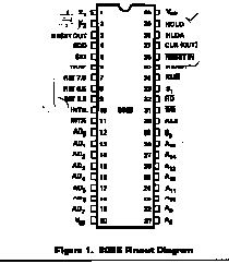
TRAP (Input)
Trap interrupt is a nonmaskable restart interrupt. It is recognized at the same time as
INTR. It is unaffected by any mask or Interrupt Enable. It has the highest priority of any
interrupt.
RESET IN (Input)
Reset sets the Program Counter to zero and resets the Interrupt Enable and HLDA flipflops.
None of the other flags or registers (except the instruction register) are affected The
CPU is held in the reset condition as long as Reset is applied.
RESET OUT (Output)
Indicates CPlJ is being reset. Can be used as a system RESET. The signal is synchronized
to the processor clock.
X1, X2 (Input)
Crystal or R/C network connections to set the internal clock generator X1 can also be an
external clock input instead of a crystal. The input frequency is divided by 2 to give the
internal operating frequency.
CLK (Output)
Clock Output for use as a system clock when a crystal or R/ C network is used as an input
to the CPU. The period of CLK is twice the X1, X2 input period.
IO/M (Output)
IO/M indicates whether the Read/Write is to memory or l/O Tristated during Hold and Halt
modes.
SID (Input)
Serial input data line The data on this line is loaded into accumulator bit 7 whenever a
RIM instruction is executed.
SOD (output)
Serial output data line. The output SOD is set or reset as specified by the SIM
instruction.
Vcc
+5 volt supply.
Vss
Ground Reference.
The 8085A is a complete 8 bit parallel central processor. It is designed with N channel
depletion loads and requires a single t5 volt supply Its basic clock speed is 3 MHz thus
improving on the present 8080's performance with higher system speed. Also it is designed
to fit into a minimum system of three IC's: The CPU, a RAM/ IO, and a ROM or PROM/IO chip.
The 8085A uses a multiplexed Data Bus. The address is split between the higher 8bit
Address Bus and the lower 8bit Address/Data Bus. During the first cycle the address is
sent out. The lower 8bits are latched into the peripherals by the Address Latch Enable
(ALE). During the rest of the machine cycle the Data Bus is used for memory or l/O data.
The 8085A provides RD, WR, and lO/Memory signals for bus control. An Interrupt Acknowledge
signal (INTA) is also provided. Hold, Ready, and all Interrupts are synchronized. The
8085A also provides serial input data (SID) and serial output data (SOD) lines for simple
serial interface.
In addition to these features, the 8085A has three maskable, restart interrupts and one
nonmaskable trap i nterrupt.
The 8085A includes the following features onchip in addition to all of the 8080A
functions.
The internal clock generator requires an external crystal or RC network. It will oscillate
at twice the basic CPU operating frequency. A 50% duty cycle, two phase, nonoverlapping
clock is generated from this oscillator internally and one phase of the clock (˘2) is
available as an external clock. The 8085A directly provides the external RDY
synchronization previously provided by the 8224. The RESET IN input is provided with a
Schmitt action input so that poweron reset only requires a resistor and capacitor. RESET
OUT is provided for System RESET.
The 8085A provides RD, WR and IO/M signals for Bus control. An INTA which was previously
provided by the 8228 in 8080 system is also included in 8085A.
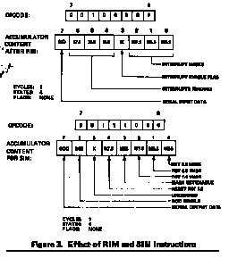
Status Information
Status information is directly available from the 8085A. ALE serves as a status stobe. The
status is partially encoded, and provides the user with advanced timing of the type of bus
transfer being done. IO/M cycle status signal is provided directly also. Decoded So, S
Carries the following status information:
HALT
WRITE
READ
FETCH
S1 can be interpreted as R/W in all bus transfers.
In the 8085A the 8 LSB of address are multiplexed with the data instead of status. The ALE
line is used as a strobe to enter the lower half of the address into the memory or
peripheral address latch. This also frees extra pins for expanded interrupt capability.
Interrupt and Serial l/O
The8085A has5 interrupt inputs: INTR, RST5.5, RST6.5, RST 7.5, and TRAP. INTR is identical
in function to the 8080 INT Each of three RESTART inputs, 5.5, 6.5. 7.5, has a
programmable mask. TRAP is also a RESTART interrupt except it is nonmaskable.
The three RESTART interrupts cause the internal execution of RST (saving the program
counter in the stack and branching to the RESTART address) if the interrupts are enabled
and if the interrupt mask is not set. The nonmaskable TRAP causes the internal execution
of a RST independent of the state of the interrupt enable or masks.
Name RESTART Address (Hex)
TRAP
RST 5.5
RST 6.5
RST 7.5
2416
2C16
3416
3C16
There are two different types of inputs in the restart interrupts. RST 5.5 and RST 6.5 are
high levelsensitive like INTR (and INT on the 8080) and are recognized with the same
timing as INTR. RST 7.5 is rising edgesensitive.
For RST 7.5, only a pulse is required to set an internal flip flop which generates the
internal interrupt request. The RST 7.5 request flip flop remains set until the request is
serviced. Then it is reset automatically. This flip flop may also be reset by using the
SIM instruction or by issuing a RESET IN to the 8085A. The RST 7.5 internal flip flop will
be set by a pulse on the RST 7.5 pin even when the RST 7.5 interrupt is masked out.
The status of the three RST interrupt masks can only be affected by the SIM instruction
and RESET IN.
The interrupts are arranged in a fixed priority that determines which interrupt is to be
recognized if more than one is pending as follows: TRAP highest priority, RST 7.5, RST
6.5, RST 5.5, INTR lowest priority This priority scheme does not take into account the
priority of a routine that was started by a higher priority interrupt. RST 5.5 can
interrupt a RST 7.5 routine if the interrupts were reenabled before the end of the RST 7.5
routine.
The TRAP interrupt is useful for catastrophic errors such as power failure or bus error.
The TRAP input is recognized just as any other interrupt but has the highest priority. It
is not affected by any flag or mask. The TRAP input is both edge and level sensitive. The
TRAP input must go high and
 remain
high to be acknowledged, but will not be recognized again until it goes low,
then high again. This avoids any false triggering due to noise or logic glitches.
The following diagram illustrates the TRAP interrupt request circuitry within
the 8085A.
remain
high to be acknowledged, but will not be recognized again until it goes low,
then high again. This avoids any false triggering due to noise or logic glitches.
The following diagram illustrates the TRAP interrupt request circuitry within
the 8085A.
Note that the servicing of any interrupt (TRAP, RST 7.5, RST 6.5, RST 5.5, INTR) disables
all future interrupts (except TRAPs) until an El instruction is executed.
The TRAP interrupt is special in that it preserves the previous interrupt enable status.
Performing the first RIM instruction following a TRAP interrupt allows you to determine
whether interrupts were enabled or disabled prior to the TRAP. All subsequent RIM
instructions provide current interrupt enable status.
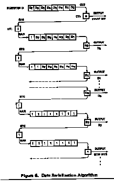
The serial l/O system is also controlled by the RIM and SIM instructions. SID is read by
RIM, and SIM sets the SOD data.
The 8085A has a multiplexed Data Bus. ALE is used as a strobe to sample the lower 8bits of
address on the Data Bus. Figure 2 shows an instruction fetch, memory read and l/ O write
cycle (OUT). Note that during the l/O write and read cycle that the l/O port address is
copied on both the upper and lower half of the address.
As in the 8080, the READY line is used to extend the read and write pulse lengths so that
the 8085A can be used with slow memory. Hold causes the CPU to relinguish the bus when it
is through with it by floating the Address and Data Buses.
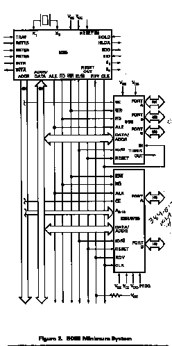
8085A family includes memory components, which are directly compatible to the 8085A CPU.
For example, a system consisting of the three chips, 8085A, 8156, and 8355 will have the
following features:
á 2K Bytes ROM
á 256 Bytes RAM
á 1 Timer/Counter
á 4 8bit l/O Ports
á 1 6bit l/O Port
á 4 Interrupt Levels
á Serial In/Serial Out Ports
This minimum system, using the standard l/O technique is as shown in Figure 3.
In addition to standard l/O, the memory mapped l/O offers an efficient l/O addressing
technique. With this technique, an area of memory address space is assigned for l/O
address, thereby, using the memory address for l/O manipulation. Figure 4 shows the system
configuration of Memory Mapped l/O using 8085A.
The 8085A CPU can also interface with the standard memory that does not have the
multiplexed address/data bus. It will require a simple 8212 (8bit latch) as shown in
Figure 5.

Return to: | Documents | 8085 |
Continue on: | Preface | CPU Functions | 8-bit family | Glossary |
11/03/97